


Feature Story
More feature stories by year:
2024
2023
2022
2021
2020
2019
2018
2017
2016
2015
2014
2013
2012
2011
2010
2009
2008
2007
2006
2005
2004
2003
2002
2001
2000
1999
1998
![]() Return to: 2016 Feature Stories
Return to: 2016 Feature Stories
CLIENT: ADESTO TECHNOLOGIES
Nov. 17, 2016: AnandTech
There is no Moore's Law for flash memory. Unlike transistors, flash memory cells can no longer be made any smaller or faster without incurring reliability tradeoffs that negate the benefits of a process shrink. This has forced the solid state storage industry to look elsewhere for potential improvements. The long-term hopes are focused on a variety of non-volatile memory technologies that are years away from reaching the cost and density of NAND flash, but promise vast improvements to endurance, latency or power consumption. In the meantime, the challenge is to reduce cost or increase the performance that is possible from flash memory by changing how it is organized and accessed.
In the PC SSD market, two major shifts are underway to satisfy the need for continued progress in spite of the stagnation of the fundamental underlying memory cell technology. 3D NAND flash is replacing planar NAND flash, enabling density to continue growing and cost per bit to decline further while keeping the memory cell large enough to provide acceptable write endurance. Further up the storage stack, PCIe and the NVMe protocol allow for substantial improvements in throughput and latency as compared with the SATA interface.
But the SSD market is hardly the only outlet for flash memory technology. 3D NAND flash is beginning to replace planar NAND in smartphones and memory cards, and faster host interfaces are available for those markets. For even smaller embedded systems, NOR flash is still used. In these markets, low power and cost are often a higher priority than capacity and performance. The increasing popularity of the Internet of Things means many of those devices now have to include full network stacks supporting IPv6 and LTE, and thus their storage requirements have increased substantially.
Adesto is one of the many companies developing a new non-volatile memory, but their conductive bridging RRAM (CBRAM) so far only offers sub-megabit capacities. Adesto's flash memory products are tailored for low-power embedded and IoT applications. Optimizing a memory product for these uses typically means using a low pin count interface like SPI and implementing extremely low-power sleep states. Erase block sizes are tuned to suit expected access patterns.
Adesto's latest family of flash memory products makes some more drastic changes. Their EcoXiP line is intended for systems with an Execute In Place (XiP) memory architecture where the processor fetches code directly from flash into the instruction cache rather than loading it into a separate DRAM or SRAM bank. XiP systems save money by requiring less RAM, but at the cost of making CPU performance highly dependent on the performance of the flash.
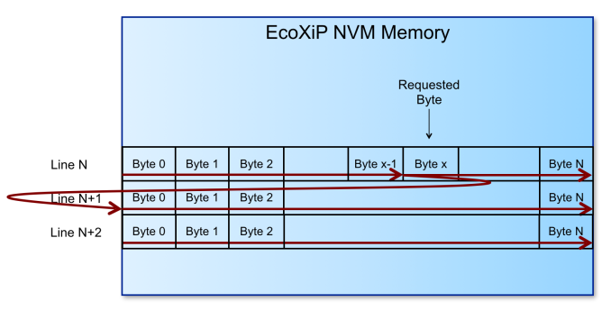
EcoXiP introduces a new mode for reading data that is designed to minimize the latency and command overhead of handling instruction cache misses. When the processor needs to branch to an address that is not in the instruction cache, it can issue a read request starting at the exact byte that is required. After the unavoidable latency of issuing the command and waiting for the flash to be read, the EcoXiP memory begins streaming the data from the requested byte. After reaching the end of the cache line the EcoXiP memory automatically wraps around to the earlier portion of the cache line so that the processor can fully populate that cache line while execution continues. The EcoXiP memory can then optionally proceed to sequentially stream subsequent cache lines in-order without requiring new read commands and addresses to be issued. Adesto estimates that the combination of delivering the most important byte first and enabling fast pre-fetching can increase effective CPU performance by over 40% for the case of a 266MHz processor using a 133MHz Octal SPI interface to flash with 100ns access time.
EcoXiP memory devices also support configuring the memory to behave as two independent banks. A single NOR flash bank cannot perform reads and writes simultaneously, which for an XiP device typically means the flash has to be treated as effectively a ROM device. Partitioning the device into separate banks allows the same chip to be used for both XiP operation and data logging, or to allow a software update to be installed to the second bank without suspending execution from the first bank.
The obvious downside to these innovations is that it is non-standard behavior. SPI itself is not a formal standard, but it is a widely supported de facto standard that has been around for decades, and JEDEC has defined a standard for querying the capabilities of SPI flash devices (similar to SPD and XMP for DRAM modules). Adesto's protocol extensions require modifications to the processor's memory controller and using EcoXiP will influence other system-level design decisions about memory and storage. Adesto has secured the support of microcontroller vendor NXP and IP vendors Synopsys and Mobiveil, so they should have no trouble building the market of devices that support EcoXiP memory.
Just as NVMe's benefits over SATA will continue to help as SSDs using new persistent memories like 3D XPoint instead of flash come to market, Adesto's protocol optimizations are not limited to just flash memory devices. Since most new persistent memory technologies will initially be available in capacities too small to directly replace NAND flash for SSD use and many of those technologies will be more economical to use as discrete memory devices rather than embedded memory integrated on SoCs, we will probably see several vendors producing specialized memory devices with optimizations similar to those used in Adesto's EcoXiP.
EcoXiP memory is initially available as a 32Mb (4MB) device rated for 100,000 Program/Erase cycles and 20 year data retention, with a maximum transfer rate of 266MB/s. Capacities up to 128Mb (16MB) are planned.
Return to: 2016 Feature Stories