


Feature Story
More feature stories by year:
2024
2023
2022
2021
2020
2019
2018
2017
2016
2015
2014
2013
2012
2011
2010
2009
2008
2007
2006
2005
2004
2003
2002
2001
2000
1999
1998
 Return to: 2015 Feature Stories
CLIENT: IDTECHEX
Aug. 21, 2015: EE Times
Dr. Khasha Ghaffarzadeh, Head of Consulting, IDTechEx
Conductive inks and pastes remain one of the largest and most dynamic sectors in printed electronics.
Conductive inks and pastes remain one of the largest sectors in the greater printed electronics market, generating $2.2 billion in 2015. IDTechEx Research forecasts this market to grow to $3 billion in 2025, as illustrated in the chart below.
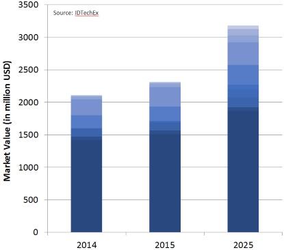
Market for conductive inks and pastes between 2014 and 2025. The data is from the IDTechEx Research report: Conductive Ink Markets 2015-2025: Forecasts, Technologies, Players.
The market for silver nanoparticles remains small, but the mood is changing. Larger companies have entered the scene, helping change a landscape that was previously in exclusive possession of small players. Some firms have exited the stage, but most have been replaced with fresh stock.
Silver nanoparticles set out to offer more performance for less cost compared to traditional pastes, but they turned out initially to be "less for more." There is now, however, a sense that they finally offer "more for same." Material prices have fallen, but $/kg/lb manufacturing costs will always remain many times higher than pastes due to the need to keep the nanoparticles de-aggregated throughout the chemical growth process.
The $/kg/lb will matter less, however, when you need less material. This is why higher silver prices would have certainly accelerated the uptake as it would force a more efficient use of silver. There is a robust and diverse application pipeline emerging, and success in one will transform the fortune of the industry. These are critical years for this industry as suppliers seek to evolve out of custom development work with select customers to large-scale volume sales.
The photovoltaic (PV) market has traditionally dominated the conductive paste market. Here, firing-type silver pastes are screen-printed atop billions of photovoltaic silicon wafers. The PV market experienced a drastic consolidation period between 2007 and 2014, causing the paste market to dip and also to consolidate. Growth is, however, now back in the underlying PV sector, causing volume demand to grow despite the gradual annual decline in silver content per wafer. The previous big boys dominated sales although there is now renewed friction on the top with heightened risk of IP battles.
The touch screen market is growing even though the uptake of large-sized touch has largely disappointed. Here, low-temperature silver paste is screen-printed as the edge electrodes. A big trend is towards narrowing the bezel even more, reducing the linewidth-to-spacing (L/S) ratio of edge (bezel) electrodes. This trend will ultimately push screen printing beyond its limits in the long term and will open the door for other printing methods.
There is also continued pressure to switch to copper-based inks to reduce cost. Here, the suppliers want to offer the "same for less." There has been tremendous effort, but copper is far behind silver in its technology learning curve, therefore technical challenges still need to be ironed out. However, we can expect rising sales figures for innovative sintering machines (machines that prevent copper oxidization) to finally open the door for the flow of copper sales. This is a space to watch closely.
A range of emerging applications are now capturing much of the attention as follows:
Wearable Electronics: Wearable electronics are now trending, so this topic is on all suppliers' agendas, including those who supply conductive inks. Many detect an opportunity in creating speciality inks that can be washed and stretched. The idea is that the printed inks can act either as interconnect or as piezo resistive sensors on textiles.
At this stage, many electronic-on-textile product concepts are being quickly prototyped and marketed by nimble, small players. Many suppliers have now set up partnerships with these small players to test out the markets. This sector is, however, far from mature, and ink suppliers need to change formulation so their inks survive tough washing, stretching, and adhesion tests. Ink suppliers are keen to enable e-textile possibilities and the race is on.

Antennas and Printed Circuit Boards: Using printing to rapidly prototype PCBs is being given a second chance. This time the market is emerging at two extreme ends: the hobbyist and the professional. In the former, small and simple machines create crude and simple (single-sided and -- more rarely -- double-sided) circuits with low conductivity and wide tracks (e.g., 500um). These machine makers raise money using crowd funding and price their products at the low end. This trend will soon fizzle out because the incumbent -- a low priced CNC machine -- offers much more for less, so the chances are that the substitute will not succeed. The consumable costs for printing will be a further handicap as will be their inability to cost-effectively create a continuous ground plane.
The professional end is a different story. Here, complex inkjet printing systems are being engineered that can deposit alternating layers of silver nanoparticle and insulting inks, thereby creating multi-layer PCBs with narrow tracks compatible with most SMDs. The target market here is rapid prototyping or low volume manufacture of boards with four layers or higher (etching PCBs gets more tricky with increasing layer numbers). This approach seeks to reduce prototyping turnaround time for multi-layer circuits while keeping all the circuit IP in house.
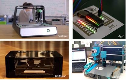
A section of low-end PCB prototyping printers.
The value proposition seems strong, but major question marks remain. The printed PCB may not have the same high frequency behaviour as the etched one. The turnaround time issue is only acute for five layers or more, and -- most importantly -- the technology itself is not yet market-ready to the extent that we can verify if it will do what it says in the tin.
Combining Printed Electronics and 3D Printing: Yet another trend is combining printed electronics and 3D printing. The idea is to weave electronics into 3D printed objects. Various approaches are being developed in parallel. Conductive filaments are improving, but they remain barely conductive, not even coming close to levels that enable useful circuits. Aerosol deposition is making good progress, but it is at its best for depositing on the final surface. Standard printed conductive inks have a high sintering temperature, often above the glass temperature of 3D plastic, while UV curing can have many side effects on polymer properties.
Structural Electronics: Molded electronics is a subset of structural electronics -- a grand trend that sees electronics disappear into the bodies of objects. Here, the idea is to put the electronics on plastic films so they can be moulded or thermoformed into 3D shapes.
This approach is best for manufacturing high volume, low-complexity circuits. Indeed, moulded electronics was once on the cusp of a fantastic success story when it was used to create a thin and sleek car overhead controller. Sadly, Ford pulled back this part soon after its launch.
The sector is, however, not dead, and it will make a comeback soon. The material armoury is expanding. Here, too, ink technology remains immature as inks have to withstand thermoforming and extreme stretching conditions. There are problems to solve, but the big marketing challenge will ultimately be developing applications that steer well away from simple low-cost mechanical switches.
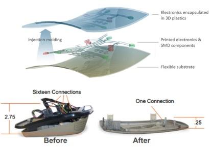
Source: Tacotek, T-Ink.
Conductive inks and pastes remain one of the largest and most dynamic sectors in printed electronics. It is often perceived that this technology is "old hat," but the industry keeps itself dynamic by offering new products and by finding new markets. The technology is not stale, even in the more mature sectors like PV, as -- here too -- cut-throat competition is pushing through rapid incremental product improvements. The strong pipeline of newly emerging market outlets also creates new requirements and opportunities. Next generation technologies, like copper or nano inks, will also progress as the existing incumbent paste technologies are expected to plateau soon, although -- thus far -- they've managed to stay ahead of the game.
Conductive inks and related topics will be covered at the IDTechEx Printed Electronics USA conference and exhibition, which will take place November 18-19, 2015, in Santa Clare, California.
Return to: 2015 Feature Stories